- 您现在的位置:买卖IC网 > Sheet目录2008 > MAX1186ECM+TD (Maxim Integrated Products)IC ADC 10BIT 40MSPS DL 48-TQFP
MAX1186
Dual 10-Bit, 40Msps, 3V, Low-Power ADC with
Internal Reference and Multiplexed Parallel Outputs
14
______________________________________________________________________________________
Applications Information
Figure 5 depicts a typical application circuit containing
two single-ended to differential converters. The internal
reference provides a VDD / 2 output voltage for level
shifting purposes. The input is buffered and then split to
a voltage follower and inverter. One lowpass filter per
ADC suppresses some of the wideband noise associat-
ed with high-speed operational amplifiers that follows
the amplifiers. The user may select the RISO and CIN
values to optimize the filter performance, to suit a par-
ticular application. For the application in Figure 5, a
RISO of 50
is placed before the capacitive load to pre-
vent ringing and oscillation. The 22pF CIN capacitor
acts as a small bypassing capacitor.
Using Transformer Coupling
An RF transformer (Figure 6) provides an excellent
solution to convert a single-ended source signal to a
fully differential signal, required by the MAX1186 for
optimum performance. Connecting the center tap of the
transformer to COM provides a VDD / 2 DC level shift to
the input. Although a 1:1 transformer is shown, a step-
up transformer may be selected to reduce the drive
requirements. A reduced signal swing from the input
driver, such as an op amp, may also improve the over-
all distortion.
In general, the MAX1186 provides better SFDR and
THD with fully differential input signals than single-
ended drive, especially for very high input frequencies.
In differential input mode, even-order harmonics are
lower as both inputs (INA+, INA- and/or INB+, INB-) are
balanced, and each of the ADC inputs only requires
half the signal swing compared to single-ended mode.
tDOB
tCL
tCH
tCLK
tDOA
tDA/B
5 CLOCK-CYCLE LATENCY (CHA), 5.5 CLOCK-CYCLE LATENCY (CHB)
A/B
CHB
D0A/B–D9A/B
D0B
CHA
D1A
CHB
D1B
CHA
D2A
CHB
D2B
CHA
D3A
CHB
D3B
CHA
D4A
CHB
D4B
CHA
D5A
CHB
D5B
CHA
D6A
CHB
D6B
CHA
CHB
CLK
OUTPUT
D0A/B–D9A/B
OE
tDISABLE
tENABLE
HIGH
IMPEDANCE
HIGH
IMPEDANCE
VALID DATA
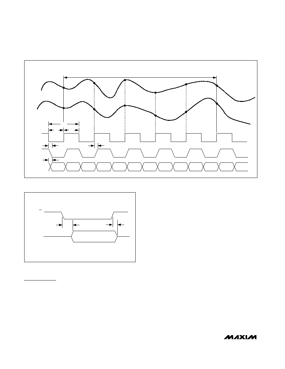
Figure 3. Timing Diagram for Multiplexed Outputs
Figure 4. Output Timing Diagram
发布紧急采购,3分钟左右您将得到回复。
相关PDF资料
MAX1187CCUI+
IC ADC 16BIT 135KSPS 28-TSSOP
MAX118EAI+
IC ADC 8BIT 1MSPS 28-SSOP
MAX1191ETI+T
IC ADC 8BIT 7.5MSPS DL 28-TQFN
MAX1192ETI+T
IC ADC 8BIT 22MSPS DL 28-TQFN
MAX1195ECM+TD
IC ADC 8BIT 40MSPS DL 48-TQFP
MAX1197ECM+TD
IC ADC 8BIT 60MSPS DL 48-TQFP
MAX1202AEPP+
IC ADC 12BIT 8CH 20-DIP
MAX121EAP+
IC ADC 14BIT 308KSPS 20SSOP
相关代理商/技术参数
MAX1186ECM-D
功能描述:模数转换器 - ADC RoHS:否 制造商:Texas Instruments 通道数量:2 结构:Sigma-Delta 转换速率:125 SPs to 8 KSPs 分辨率:24 bit 输入类型:Differential 信噪比:107 dB 接口类型:SPI 工作电源电压:1.7 V to 3.6 V, 2.7 V to 5.25 V 最大工作温度:+ 85 C 安装风格:SMD/SMT 封装 / 箱体:VQFN-32
MAX1186ECM-TD
功能描述:模数转换器 - ADC RoHS:否 制造商:Texas Instruments 通道数量:2 结构:Sigma-Delta 转换速率:125 SPs to 8 KSPs 分辨率:24 bit 输入类型:Differential 信噪比:107 dB 接口类型:SPI 工作电源电压:1.7 V to 3.6 V, 2.7 V to 5.25 V 最大工作温度:+ 85 C 安装风格:SMD/SMT 封装 / 箱体:VQFN-32
MAX11871GTM+T
制造商:Maxim Integrated Products 功能描述:
MAX1187ACUI
功能描述:模数转换器 - ADC RoHS:否 制造商:Texas Instruments 通道数量:2 结构:Sigma-Delta 转换速率:125 SPs to 8 KSPs 分辨率:24 bit 输入类型:Differential 信噪比:107 dB 接口类型:SPI 工作电源电压:1.7 V to 3.6 V, 2.7 V to 5.25 V 最大工作温度:+ 85 C 安装风格:SMD/SMT 封装 / 箱体:VQFN-32
MAX1187ACUI+
功能描述:模数转换器 - ADC 16-Bit 135ksps 4.2V Precision ADC RoHS:否 制造商:Texas Instruments 通道数量:2 结构:Sigma-Delta 转换速率:125 SPs to 8 KSPs 分辨率:24 bit 输入类型:Differential 信噪比:107 dB 接口类型:SPI 工作电源电压:1.7 V to 3.6 V, 2.7 V to 5.25 V 最大工作温度:+ 85 C 安装风格:SMD/SMT 封装 / 箱体:VQFN-32
MAX1187ACUI+T
功能描述:模数转换器 - ADC 16-Bit 135ksps 4.2V Precision ADC RoHS:否 制造商:Texas Instruments 通道数量:2 结构:Sigma-Delta 转换速率:125 SPs to 8 KSPs 分辨率:24 bit 输入类型:Differential 信噪比:107 dB 接口类型:SPI 工作电源电压:1.7 V to 3.6 V, 2.7 V to 5.25 V 最大工作温度:+ 85 C 安装风格:SMD/SMT 封装 / 箱体:VQFN-32
MAX1187ACUI-T
功能描述:模数转换器 - ADC RoHS:否 制造商:Texas Instruments 通道数量:2 结构:Sigma-Delta 转换速率:125 SPs to 8 KSPs 分辨率:24 bit 输入类型:Differential 信噪比:107 dB 接口类型:SPI 工作电源电压:1.7 V to 3.6 V, 2.7 V to 5.25 V 最大工作温度:+ 85 C 安装风格:SMD/SMT 封装 / 箱体:VQFN-32
MAX1187AEUI
功能描述:模数转换器 - ADC RoHS:否 制造商:Texas Instruments 通道数量:2 结构:Sigma-Delta 转换速率:125 SPs to 8 KSPs 分辨率:24 bit 输入类型:Differential 信噪比:107 dB 接口类型:SPI 工作电源电压:1.7 V to 3.6 V, 2.7 V to 5.25 V 最大工作温度:+ 85 C 安装风格:SMD/SMT 封装 / 箱体:VQFN-32